Author: Yawei Lv
School of Physics and Technology, Wuhan University
lvyawei@whu.edu.cn

In this tutorial, the transport properties of SNW [1] are simulated based on the multi-scale method [2] in tutorial 14. The ab-initio calculation package Quantum Espresso and transformation package Wannier90 are adopted to get the TB Hamiltonian. Compared with the GNR, the spread of the orbitals in silicon is wider, so, more interactions between different orbitals are retained: the computation complexity is increased as well. The RAM adopted in this tutorial is at least 16G. And we recommend the readers to use a CPU which is more powerful than Intel Core I7 processor.
We assume that the readers have already installed the needed packages and the simulation scheme is shown as below.
The needed files can be downloaded here (All the files come from tutorial 14 except for ‘NanoTCAD_ViDES.py’, and they have been revised to carry out this simulation. More details about the revision can be found in ‘README’).
- Set the correct environment variables.
- ./run_QE run the “relax” and “nscf” calculation to get the band structure of the SNW with force relaxing.
- Run ‘gfortran Wannier2ViDES.f90 –o Wannier2ViDES’ to get software which is used to generate the final TB Hamiltonian. Copy the executable to the bin file of Quantum Espresso, for example ‘/home/XXX/espresso-5.0.2/bin’
- ./run_Wannier get the TB Hamiltonian transformed by Wannier function. The DOS property can also be got in this step.
The final files we need are ‘wannier_center.xyz’ which contains the position of Wannier functions, the Hamiltonian file ‘Wannier2ViDES.H’, and ‘n_Nc.dat’ which contains n and Nc used in the Hamiltonian command. We have included all these three files in the tutorial and the readers can directly run NanoTCAD without Quantum Espresso and Wannier90. Before the transport property calculation using NanoTCAD ViDES, we have modified the code in order to define a cylindrical region. As a consequence, either put the new file ‘NanoTCAD_ViDES.py’ in the installation directory, or directly in the directory you run simulations. (‘NanoTCAD_ViDES.py’ file is contained in the .zip file)
Now let’s begin the simulation.

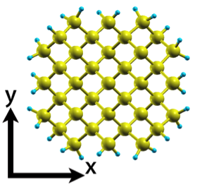
The structure of the device is depicted above. The length of the SNW is 20nm and it is covered by the SiO2 layer with the thickness of 1nm. The source and drain regions are all 5nm and the gate is wrapped around the channel region. The doping concentration is 1 × 10⁻² Coulomb per silicon atom.
Vgsmin=0.00;
Vgsmax=1.30;
Vgstep=0.1;
num=int(round((Vgsmax-Vgsmin)/Vgstep)+1);
Si=region(“cyl”,1.13196786,1.13196786,0,0.6277,grid.zmin,grid.zmax);
Si.eps=11.8;
SiO2=region(“cyl”,1.13196786,1.13196786,0,1.6277,grid.zmin,grid.zmax);
SiO2.eps=3.9;
SNW.Elower=-1;
SNW.Eupper=1;
z1=grid.zmin+5;
z2=grid.zmax-5;
gate=gate(“cyl”,1.13196786,1.13196786,0,2.1277,z1,z2)
offset=0;
gate.Ef=-Vgsmin;
p=interface3D(grid,SiO2,Si,gate);
p.underel=0.5
p.normpoisson=1e-3;
source_dope=region(“cyl”,1.13196786,1.13196786,0,0.6277,grid.zmin,z1);
drain_dope=region(“cyl”,1.13196786,1.13196786,0,0.6277,z2,grid.zmax);
dope_reservoir(grid,p,SNW,1e-2,source_dope);
dope_reservoir(grid,p,SNW,1e-2,drain_dope);
The parameters in the region command in sequence are the region type (‘cyl’ means cylinder), the x and y coordinates of the axes. The cylinder can be hollow and the fourth and fifth parameters are the inner diameter and outer diameter. And the last two parameters define the length of the cylinder.
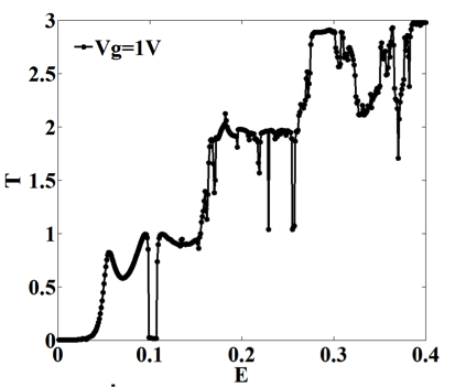
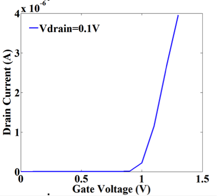
The transfer property is calculated from 0 to 1.3V in this script. The resulting current curve and transmission coefficients are displayed below.
References
If you use this script please cite:
[1] Y. Lv, H. Wang, S. Chang, J. He, and Q. Huang, “Band Structure Effects in Extremely Scaled Silicon Nanowire MOSFETs With Different Cross Section Shape,” Electron Devices, IEEE Transactions on, vol. PP, no. 99, pp. 1-1, 2015.
[2] S. Bruzzone, G. Iannaccone, N. Marzari, and G. Fiori, “An Open-Source Multiscale Framework for the Simulation of Nanoscale Devices,” Electron Devices, IEEE Transactions on, vol. 61, no. 1, pp. 48-53, 2014.
and the NanoTCAD ViDES code as:
[3] G Fiori, G Iannaccone ‘Multiscale Modeling for Graphene-Based Nanoscale Transistors’ Proceedings Of The IEEE, Vol. 101, p. 1653-1669, 2013.