
Simulating Silicene FET is straightforward starting from the graphene class, which has to be slightly changed.
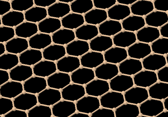
According to L C Lew Yan Voon and A Lopez-Bezanilla and J Wang and Y Zhang and M Willatzen, “Effective Hamiltonians for phosphorene and silicene”, New Journal of Physics, Vol. 17, p. 025004, 2015, Silicene bands are similar to graphene bands (i.e., Dirac cone in correspondence of the K point), but with a different Fermi velocity and a different lattice constant. If we assume valid a tight-binding Hamiltonian approximating the linear dispersion in the K point, we can compute the new hopping parameters and the new atom-to-atom distance as thop=0.735 eV and aCC=0.384 nm, respectively. We can then change accordingly the class graphene, so to simulate Silicene.
Let’s suppose, we want to simulate a double-gate silicene FET with channel length equal 20 and 10 nm for each doped reservoirs. The total length for the device is then 40 nm.
Taking into account that aCC=0.144 nm for graphene, Silicene class is the following (considering the scaling factor):
 Silicene=graphene(15.5);
 acc=0.384;
 Silicene.acc=acc;
 Silicene.thop=0.735;
 Silicene.delta=sqrt(3)*acc;
 Silicene.y=Silicene.y/0.144*acc;
 Silicene.kmax=pi/Silicene.delta;
 Nky=32;
 Silicene.kmax=pi/Silicene.delta;
 Silicene.dk=Silicene.kmax/Nky
Then the script for the computation of the transfer characteristics is the same for any other materials.
The complete script can be found here.