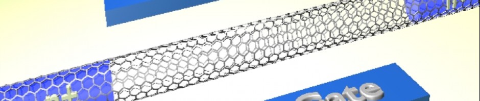
We now want to consider a (13,0) CNT, 10 nm long, embedded in SiO2, with
top and bottom oxide thickness equal to 0.5 nm and lateral spacing equal to 0.5 nm.
We also consider a top and a bottom gate: the top gate is biased at 0.1 V, and the bottom gate
is biased at 0 V.
Let’s first load the module
from NanoTCAD_ViDES import *
and then create the CNT
CNT=nanotube(13,10);
We then create the grid, accordingly to the above specifics
xg=linspace(-1,1,20);
yg=xg;
grid=grid3D(xg,yg,CNT.z,CNT.x,CNT.y,CNT.z);
I can also save the computed grid along the different directions
in three different files “gridx.out”, “gridy.out” and “gridz.out”
savetxt(“gridx.out”,grid.gridx);
savetxt(“gridy.out”,grid.gridy);
savetxt(“gridz.out”,grid.gridz);
Let’s now take care of the top and bottom gates
top_gate=gate(“hex”,1,1,-1,1,grid.gridz[0],grid.gridz[grid.nz-1])
bottom_gate=gate(“hex”,-1,-1,-1,1,grid.gridz[0],grid.gridz[grid.nz-1])
As can be seen, both top and bottom gates are placed over the whole CNT, so that zmin=grid.gridz[0] and zmax=grid.gridz[grid.nz-1]
We need to fix the Fermi level of both gates
top_gate.Ef=-0.1;
bottom_gate.Ef=0;
as well as to define the SiO2 region, embedding the CNT
SiO2=region(“hex”,-1,1,-1,1,0,grid.gridz[grid.nz-1]);
SiO2.eps=3.9;
We also need to define the interface
p=interface3D(grid,top_gate,bottom_gate,SiO2);
p.normpoisson=1e-1;
Here the norm of the variance of the potential computed in the solve_Poisson function has been set to 10-1.
We then can solve the Poisson equation. Actually, in this example the free charge has not been specified, but only initialized but the instance, and imposed to zero. As a consequence, the Laplace equation is solved.
solve_Poisson(grid,p);
At this point, the solution of the Laplace equation is stored in p.Phi.
We can now for example pass this potential to the CNT, and compute the charge.
To do this, we need the p.swap array. As shown in the nanoribbon session, the CNT.Phi potential is an array of double n*Nc long, while the electrostatic potential is defined along the whole grid, so p.Phi is an array of double, whose dimension is Np. In addition, elements in CNT.Phi are not ordered as in p.Phi. To solve this problem, we need an array of indexes, which maps points of the 3D grid, to point of the CNT. Such a function is done by the p.swap array.
In particular,
CNT.Phi=p.Phi[grid.swap];
We can now compute the charge and the transmission coefficient of the CNT
CNT.charge_T();
We can also plot the potential, previously computed by solve_Poisson
section(“z”,p.Phi,5,grid)
Here the complete listing of the python script
from NanoTCAD_ViDES import *
#I create the (13,0) CNT, 10 nm long
CNT=nanotube(13,10);
#I create the grid
xg=linspace(-1,1,20);
yg=xg;
grid=grid3D(xg,yg,CNT.z,CNT.x,CNT.y,CNT.z);
#I save the computed grid
savetxt(“gridx.out”,grid.gridx);
savetxt(“gridy.out”,grid.gridy);
savetxt(“gridz.out”,grid.gridz);
# Now I define the gate regions
# The device is a double gate and the oxide thickness is
# equal to 0.5 nm
# The lateral spacing is 0.5 nm, too
top_gate=gate(“hex”,1,1,-1,1,grid.gridz[0],grid.gridz[grid.nz-1])
bottom_gate=gate(“hex”,-1,-1,-1,1,grid.gridz[0],grid.gridz[grid.nz-1])
top_gate.Ef=-0.1;
bottom_gate.Ef=0;
# I take care of the region embedding the CNT, which is SiO2
SiO2=region(“hex”,-1,1,-1,1,0,grid.gridz[grid.nz-1]);
SiO2.eps=3.9;
# I then define the interface
p=interface3D(grid,top_gate,bottom_gate,SiO2);
p.normpoisson=1e-1;
# Actually the charge term is imposed to zero, so I
# solve the Laplace equation
solve_Poisson(grid,p);
# I pass the computed potential to the CNT instance.
# Note that the I need to grid.swap array to map points
# in the 3D domain, to points belonging to the CNT domain
CNT.Phi=p.Phi[grid.swap];
CNT.charge_T();
section(“z”,p.Phi,5,grid);