E-MRS Symposium Z on 2D materials

Symposium Z: Two-dimensional crystals and van der Waals heterostructures for nanoelectronics

organized by A. Molle (CNR-IMM, Italy), C. Casiraghi (Univ. Manchester, UK), A. Castellanos-Gomez (IMDEA, Spain), G. Fiori (Univ. Pisa, Italy)
at the next E-MRS 2016 Spring Meeting – Lille (France), May 2016, 2-6

Submission Deadline    January 15th, 2016
submission at http://www.european-mrs.com/meetings/2016-spring-meeting

Scope        Starting from the relatively recent rise of graphene, the family of two dimensional (2D) materials is rapidly expanding not only by including
new elements and compounds, but also by paving the way to new functionalities and applications.
Novel methods for the synthesis and functionalization are demanding to foster the 2D materials evolution,
which will be the platform for future enabling technologies.

Hot Topics    The Symposium Z is intended to highlight the most recent advances on 2D materials and their applications.
A large variety of 2D atomic crystals isolated in the recent years offers a rich platform for the creation of heterostructures,
which combine several of these materials in one stack. Among the topics that will be covered in the Symposium one can highlight:
•  Synthesis, characterization and structural controls of 2D materials (mostly transition metal dichalchogenides) and 2D van der Waals heterostructures
•  Electronic and spin transport in 2D materials
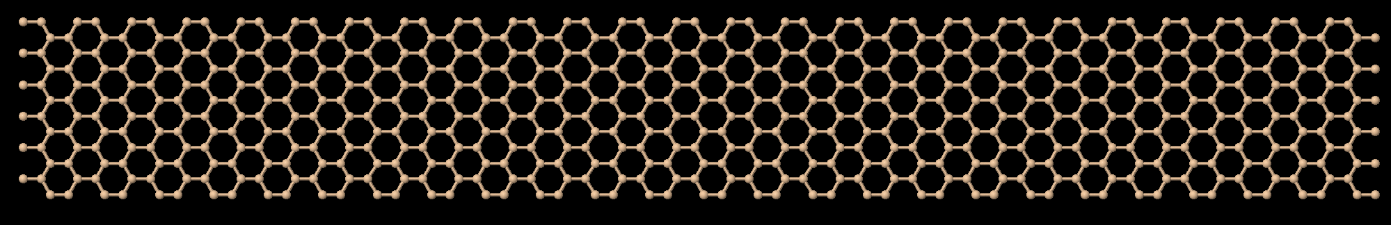
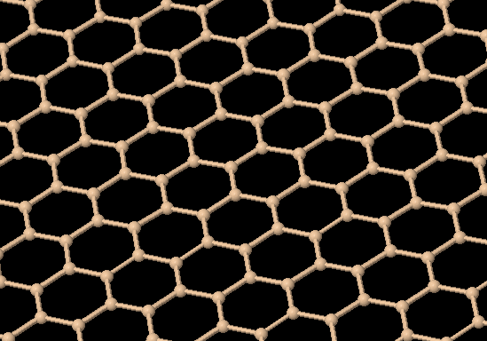
•  Novel 2D honeycomb materials: silicene, germanene, stanene, phosphorene
•  Electronic, magnetic, optical properties of 2D materials
•  Thermoelectrics, straintronics, and valleytronics in 2D materials
•  2D Materials for energy harvesting and photonics
•  2D Materials for sensor and MEMS devices
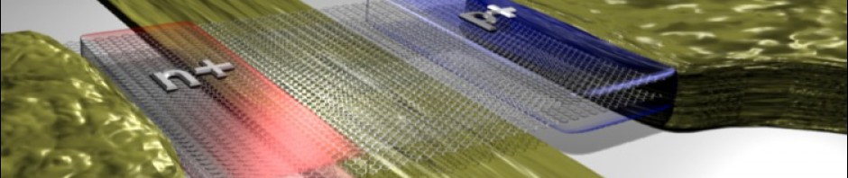
•  2D materials for Post-Si and III-V technology: Digital, Analog (RF) and flexible electronic applications
•  Advanced characterization for 2D materials

Joint sessions with the parallel Symposium “Graphene and Related Materials: from Fundamental Science to Applications”
will be eventually taken into account. Selected oral contribution(s) can be upgraded to invited talks.

A Special Issue of the Symposium Z proceedings will be published in Physica Status Solidi – Rapid Research Letters (Wiley)
upon peer-reviewed submission open to all the symposium contributors.
Upon courtesy of Wiley, a limited number of selected papers may be upgraded for publication in Advanced Electronic Materials (Wiley).

Awards:
a) Graduate Student Awards (GSA) in recognition of academic achievement and research excellence
(see http://www.emrs-strasbourg.com for details);
b) Poster Award(s) sponsored by Wiley.

Invited Speakers: R. Gorbachev (Univ. of Manchester, UK), M. Chhowalla (Rutgers Univ., USA), J. Coleman (Trinity College, Ireland),
A. Kis (EPFL, Switzerland), D. Akinwande (Univ. Texas, USA), M. Houssa (KU Leuven, BE), S. Roche (Unicat, Spain), E. Pop (Stanford Univ., USA),
F. Koppens
(ICFO, Spain), M. Lemme (Siegen Univ., Germany), J. Garrido (Walter Schottky Institute and Munich Univ., Germany),
F. Schwierz
(Univ. of Illmenau, Germany), D. Neumaier (AMO, Germany), M. Ugeda (CIC Nanogune, Spain), H. Zhang (Nanyang Technol. Univ., Singapore).

More info at: http://www.european-mrs.com/2016-spring-symposium-z-european-materials-research-society

The Symposium Z Organizers

Posted in Uncategorized | Leave a comment

New tutorial on multi-scale simulations of Si Nanowire Transistor

f3 f1


A new tutorial on Silicon Nanowire Transistor based on multi-scale simulations has been released and can be found here:

http://vides.nanotcad.com/vides/documentation/tutorials/tutorial-19-multi-scale-simulation-of-silicon-nanowire-transistors

The approach is based on DFT calculations of the bands through Quantum Espresso, the calculation of the tight-binding like by means of
Wannier 90 and transport calculations through NanoTCAD ViDES.

The provided script has eventually led to the following publication:

Y. Lv, H. Wang, S. Chang, J. He, and Q. Huang, “Band Structure Effects in Extremely Scaled Silicon Nanowire MOSFETs With Different Cross Section Shape,” Electron Devices, IEEE Transactions on, vol. PP, no. 99, pp. 1-1, 2015.

Posted in Uncategorized | Comments Off on New tutorial on multi-scale simulations of Si Nanowire Transistor

Tutorial on Silicene Nanoribbon

A new tutorial on Silicene Nanoribbon field effect transistor has been created and can be found here:

http://vides.nanotcad.com/vides/documentation/tutorials/tutorial-18-silicene-nanoribbon

Have fun!

GNR_plot


Posted in Uncategorized | Leave a comment

Tutorial on Transition Metal Dichalcogenides-based FET

A new tutorial has been released on TMD-based FET. In particular, the NanoTCAD ViDES code has been further extended in order to perform simulation of transition metal dichalcogenides based transistors, as MoS2, MoSe2 etc.

Detailed information can be found here:

http://vides.nanotcad.com/vides/documentation/tutorials/tutorial-17-transition-metal-dichalcogenides-based-fet

Posted in Uncategorized | Leave a comment

New Tutorial on Silicene Transistor

A new tutorial has been released and concerned with the simulation of Silicene transistor. In particular, the script of the transfer characteristic is documented and commented at: http://vides.nanotcad.com/vides/documentation/tutorials/tutorial-16-silicene-transistor Screen Shot 2015-07-30 at 4.32.29 PM

Posted in Uncategorized | Leave a comment

Release of the Beta version of the IDE for NanoTCAD ViDES

The evaluation version of the IDE for the NanoTCAD ViDES code has been released today.

The easy-to-use IDE integrates a GUI interface to define and simulate in a simple fashion nanoscale devices, including monolayer transition metal dichalcogenides based Field Effect Transistors.

As of now, the beta version is a binary file, which works for 64bit Linux operating systems and already include the NanoTCAD ViDES module (no need for additional installation).

Complete information (quick start guide, screenshots, download, installation and activation of the IDE) can be found in the vIDEs page of the website, at the following address: http://vides.nanotcad.com/vides/vides


Posted in Uncategorized | Leave a comment

Tutorial on 2D Materials at IEEE Nano 2015 (27th July)

A tutorial on 2D materials will be given 27th July at IEEE Nano 2015, held in Rome [link]. The abstract of the tutorial can be found below. Within the tutorial, the potential of the NanoTCAD ViDES code for the simulation of 2D materials Field Effect Transistors will be discussed, and the new IDE with GUI will be launched.

Abstract

The research community has great expectations for 2D materials, since they represent one of the most promising options towards the flexible electronics revolution. However, many issues still remain unsolved, and the set of materials is very broad and poorly characterized. Therefore, simulation-based investigations are a powerful tool in order to guide and inform progress in the field.

This tutorial will focus on electron devices based on 2D-materials, on the assessment of their expected performance, and on technology exploration through numerical simulations.

Several devices based on 2D-materials have indeed already been proposed, fabricated, and measured in experiments. However, a lot of work is needed to evaluate their possible performance in electronic systems, and their compliance with Semiconductor Industry requirements for the next 15 years.

Within this tutorial, we will first provide an overview of state-of-the-art devices based on 2D materials, ranging from digital (high-performance and low-power devices), to analog (i.e., radio frequency applications) as well as opto-electronics applications. We will then discuss the physical models suitable to describe the electrical behavior of 2D-devices (e.g., classical and quantum transport models), which will be then exploited in order to provide performance projections. Finally, we will propose some simple simulations to be run by means of the open-source NanoTCAD ViDES code.

Summary

1)   Electron devices based on 2D materials: State of the art

2)   Modeling of devices based on 2D materials:

– Semiclassical models

– Quantum transport models: the NEGF approach

3)   Assessment of device performance through device modeling

4)   Simulations of 2D-materials through the NanoTCAD ViDES code.


Posted in Uncategorized | Leave a comment

Opening of PhD and Post-doc positions

PhD/post-doc positions are opening at the University of Pisa.
The research activity will focus on the investigation of the potential of heterostructures based on Transition Metal Dichacogenides and other classical semiconductors like Silicon for opto-electronics devices.
This activity will be performed within the GRAPHENE FLAGSHIP project.
Potential candidates must have good programming skills (C, Fortran and Python), and good background in device physics.
Expressions of interest with attached detailed CV should be sent by March, 31 to both email addresses indicated below:
Gianluca Fiori
University of Pisa
Giuseppe Iannaccone
University of Pisa
giuseppe.iannaccone(at)iet.unipi.it
Posted in Uncategorized | Leave a comment

Available contract for the development of a GUI for NanoTCAD ViDES

The activity consists in the development of a GUI for the NanoTCAD ViDES code.
Potential candidates must have good programming skills (C, Fortran and Python).
Good background in device physics can represent an added value.
Work is estimated to be completed in 2 month full time equivalent of a skilled programmer.
The activity can be performed remotely, with interaction through online collaboration tools.
Payment is done as a lump sum at the end of the work.
Send enquiries, CV and examples of previous work to
Gianluca Fiori
University of Pisa
Giuseppe Iannaccone
University of Pisa
giuseppe.iannaccone(at)iet.unipi.it
Posted in Uncategorized | Leave a comment

Available contract for the development of graphene-based Organic Photovoltaic Solar Cell Simulator

The activity consists in the development of the models describing the physics in organic photovoltaic solar cells, to be included in the device simulator NanoTCAD ViDES.
In particular, the equations to be developed will include 1D Continuity equation + 1D exciton equation to be solved self-consistently with 1D Poisson equation (already implemented in the code).
Potential candidates must have good programming skills (C, Fortran and Python), and good background in device physics.
Work is estimated to be completed in 1 month full time equivalent of a skilled programmer.
The activity can be performed remotely, with interaction through online collaboration tools.
Payment is done as a lump sum at the end of the work.
Send enquiries, CV and examples of previous work by January 2014 to
Gianluca Fiori
University of Pisa
Giuseppe Iannaccone
University of Pisa
giuseppe.iannaccone(at)iet.unipi.it
Posted in Uncategorized | Leave a comment